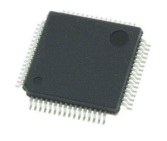
CDCLVP215RHBR
CDCLVP215RHBR Clock Buffer Dual 1:5 Hi Spd LVPECL Fan Out Bfr is an IC used in electronic systems to distribute clock signals to multiple components or circuits.
Inquire Now
Description
CDCLVP215RHBR Clock Buffer Dual 1:5 Hi Spd LVPECL Fanout Bfr, also known as Clock Distribution Buffer. An integrated circuit (IC) in an electronic system. Used to distribute a clock signal to multiple components or circuits.
The term "dual channel" in the name means that the buffer has two input channels. Each channel can distribute a clock signal to up to five output channels. The "1:5" ratio indicates that each input clock signal is divide into five identical output signals.
This buffer is design for high speed operation. And use LVPECL (Low Voltage Positive Emitter Coupled Logic) signaling. This is a differential signal used in high-speed digital circuits. The buffer also includes fan-out functionality. This means that each output channel can drive a load with minimal signal attenuation or delay.
In general, clock buffer dual 1:5 high-speed LVPECL fan-out Bfr is require for precise and synchronous clock signals. A useful component in an electronic system so that it can function efficiently.
CDCLVP215RHBR feature
- Dual input channels: The buffer has two input channels. Can be use to distribute two different clock signals or to provide redundancy if one input fails.
- 1:5 ratio: Each input clock signal is divide into five identical output signals. Can be use to drive multiple components or circuits.
LVPECL signaling: The buffer uses LVPECL signaling. This is a differential signal that provides high-speed data transmission and noise immunity. - High-speed operation: This buffer is design for high speed operation. Typical clock frequencies range from hundreds of megahertz to several gigahertz.
- Fan-out capability:Thanks to the buffer's fan-out capability. Each output channel can drive loads with minimal signal attenuation or delay.
- Low jitter: The buffer has low jitter. This is a measure of the timing variation between the input and output clock signals. Low jitter ensures that the distributed clock signals remain synchronized and stable.
- Output enable/disable: Buffers often include output enable/disable functionality. Allows the user to turn off specific output channels to save power or avoid interfering with other circuits.
FAQ
Q:What is the purpose of a CDCLVP215RHBR?
A:CDCLVP215RHBR is use to distribute a clock signal to multiple components or circuits in an electronic system. It ensures that distributed clock signals remain synchronized and stable. This is critical to the proper functioning of the system.
Q:What is LVPECL signaling?
A:Low voltage positive emitter coupled logic is a type of differential signaling used in high speed digital circuits. It provides high-speed data transmission and noise immunity. By using a voltage swing much larger than the logic threshold.
Q:What is a fan-out capability?
A:Fan-out capability refers to the ability of a buffer to drive multiple loads with minimal signal degradation or delay. In the case of a CDCLVP215RHBR, each output channel can drive up to five loads.
Q:What is jitter?
A:Jitter is a measure of the variation in timing between the input and output clock signals. Low jitter ensures that the distributed clock signals remain synchronized and stable.
Q:What is an output enable/disable feature?
A:The output enable/disable function allows the user to turn off specific output channels. To save power or avoid interfering with other circuits


